

[ad_1]
When the house laptop revolution arrived, it stuffed my childhood with fascination and impressed me to check laptop engineering. I needed to design a microcomputer to my very own specs. However at college I used to be by no means taught how a whole laptop system was put collectively. As a substitute we studied numerous subsystems and the idea of issues like digital sign processing and so forth. Anyone, some place else, would all the time be chargeable for assembling the entire system and making all the pieces work collectively.
This was unlucky and unjustified: Placing a whole working laptop collectively isn’t troublesome, and it may give college students important early confidence of their means to dwell as much as the label “laptop engineer.” So, having not too long ago retired from the high-tech trade, I made a decision to design a didactical however absolutely purposeful laptop that would function a platform for studying and experimenting with system-level design points—the Cerberus 2100.
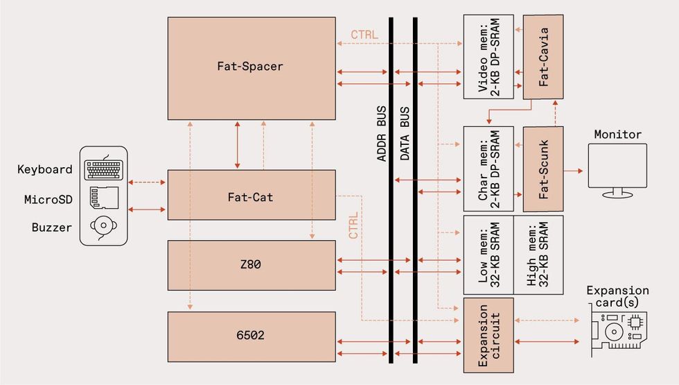
I didn’t wish to commit Cerberus to a specific CPU, as doing so would conflate system-level structure ideas with the particular timings and management alerts of that CPU. A lot as a software-engineering course focuses on the construction of an algorithm moderately than the syntax of its implementation in a specific language, I needed Cerberus to give attention to the system-level construction. Cerberus is thus a multi-CPU system, that includes each a Z80 and a W65C02S (6502), two well-known workhorse 8-bit processors that featured prominently within the home-microcomputer period. There’s a wealth of assets accessible for studying methods to program these processors, that are highly effective sufficient to be helpful and entertaining, but easy sufficient to grasp.
The issue, in fact, is that these two CPUs function with very totally different interfaces to different components of the pc, akin to reminiscence or enter/output units. As an example, the 6502 makes use of a single management line to point whether or not it’s studying or writing to the information bus, whereas the Z80 makes use of two strains. This implies the 6502’s sign must be mixed with the sign from the system clock, through an AND gate, to stop reminiscence miswrites, whereas the Z80 has no such situation. Additionally, the Z80 has an output line to sign that the worth on the tackle bus is secure, a operate absent within the 6502. And so forth.
These variations imply that I couldn’t use a normal management bus within the Cerberus. As a substitute, I used a big advanced programmable logic gadget (CPLD) chip I dubbed “Fats-Spacer” to translate the management alerts of every CPU into an abstraction layer. This layer defines the system structure. Fats-Spacer then interprets the output of the abstraction layer into the suitable enter alerts for every element within the system. These two steps of translation entail each Boolean logic and timing management via flip-flops. I used a CPLD as a substitute of an FPGA (field-programmable gate array) as a result of, in contrast to FPGAs, CPLDs have a set propagation delay whatever the Boolean logic carried out in them. That is important as a result of it permits customers to make adjustments to the system structure—by reprogramming the CPLD—with out having to fret that the complexity of their adjustments will take too lengthy to go via a sequence of logic gates, and so miss the timing home windows imposed by the system clock.
Due to its inner abstraction layer, Cerberus is uniquely appropriate for growth: A direct reminiscence entry (DMA) growth port can be linked to Fats-Spacer. By straight permitting entry to system reminiscence, I let the consumer add much more CPUs and microcontrollers to the system through the growth port.
One other important design problem was to decouple the logic of the pc from the timings of the video circuitry
One other important design problem I confronted was to decouple the system-level logic of the pc from the timings of the video circuitry. Historically, these two are tightly tied collectively in order to coordinate entry to video and character recollections by the CPU and show circuitry with out inflicting conflicts or artifacts. However with two CPUs and the DMA growth port, this wasn’t an possibility.
As a substitute, Cerberus makes use of two dual-ported static RAMs (SRAMS) as video and character recollections. Every port permits asynchronous entry to the reminiscence’s contents. One port of every SRAM is linked to the pc correct, whereas the opposite is unique to the video circuitry.
 The Z80 and 6502 processors use totally different management alerts to interface with reminiscence and interface chips. A reprogrammable logic chip, dubbed Fats-Spacer interprets these alerts as required. One other reprogrammable logic chip handles storage and the keyboard interface, whereas a 3rd generates video alerts. James Provost
Regardless of the dual-ported recollections, onscreen glitches might nonetheless occur if the video circuitry was to learn from a given tackle as the pc wrote to that very same tackle. Happily, dual-ported SRAMs present a “BUSY” sign to point a battle. This sign is utilized by Fats-Spacer to pause the CPUs at some stage in the battle. The management abstraction layer comes very helpful right here too, because it already has the suitable translation logic for pausing the CPUs.
Fats-Spacer isn’t the one CPLD in Cerberus: Three of them represent the system’s core chipset. Fats-Cavia constantly scans the video and character recollections, and sends bitmaps to Fats-Scunk, which then generates the suitable RGB alerts and synchs pulses to create a 320-by-240-pixel VGA output. In the meantime, as we’ve seen, Fats-Spacer supplies the glue logic. Lastly, there’s a further chip: Fats-Cat, which is definitely an ATmega328PB microcontroller. That is used to deal with I/O: The microcontroller manages a keyboard, buzzer, the growth protocol, and a microSD card for storage. The I/O firmware is held within the ATmega’s reminiscence, which means it leaves no reminiscence footprint within the 64 kilobytes of RAM accessible to the Z80 and 6502.
The Cerberus 2100 is an open {hardware} design accessible to all and full particulars can be found on my web site. However for many who don’t wish to construct their very own machine from scratch, I’m working with European electronics firm Olimex for the sale of a totally assembled model shortly. I hope it helps college students and hobbyists to grasp—and college to show—how a whole, absolutely purposeful laptop could be put collectively, whatever the goal CPU.
This text seems within the November 2023 print situation as “Software program-Outlined Structure.”
From Your Website Articles
Associated Articles Across the Internet
[ad_2]