(Nanowerk Information) Supplies simply atoms in thickness, referred to as two-dimensional (2D) supplies, are set to revolutionize future expertise, together with within the electronics trade. Nonetheless, commercialization of gadgets that include 2D supplies has confronted challenges as a result of problem in transferring these extraordinarily skinny supplies from the place they’re made onto the system.
Now, a analysis staff from Kyushu College, in collaboration with Japanese firm Nitto Denko, have developed a tape that can be utilized to stay 2D supplies to many various surfaces, in a straightforward and user-friendly manner.
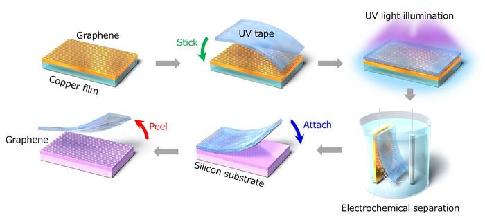
The tape adjustments its ‘stickiness’ to 2D supplies resulting from UV mild. (Picture: In the past Lab, Kyushu College)
“Transferring 2D supplies is often a really technical and complicated course of; the fabric can simply tear, or grow to be contaminated, which considerably degrades its distinctive properties,” says lead creator, Professor Hiroki In the past of Kyushu College’s International Innovation Heart. “Our tape provides a fast and easy various, and reduces injury.”
The researchers started by specializing in graphene. Constituted of a skinny sheet of carbon atoms, graphene is hard, versatile, and lightweight, with excessive thermal and electrical conductivity. Dubbed a “marvel materials” upon discovery, it has potential purposes in biosensing, anti-cancer drug supply, aeronautics and digital gadgets.
“One of many predominant strategies of creating graphene is thru chemical vapor deposition, the place graphene is grown on copper movie. However to carry out correctly, the graphene have to be separated from the copper and transferred onto an insulating substrate, like silicon,” Professor In the past explains. “To do that, a protecting polymer is positioned over the graphene, and the copper is then eliminated utilizing etching resolution, reminiscent of acid. As soon as connected to the brand new substrate, the protecting polymer layer is then dissolved with a solvent. This course of is expensive, time-consuming and may trigger defects to the graphene’s floor or go away traces of the polymer behind.”
Professor In the past and his colleagues due to this fact aimed to supply an alternate manner of transferring graphene. They used AI to develop a specialised polymer tape, dubbed “UV tape”, which adjustments its attraction to graphene when irradiated with UV mild.
Earlier than publicity to UV mild, the tape has a robust adhesion to graphene, permitting it to “stick”. However after UV publicity, the atom bonding adjustments, which decreases the extent of adhesion to graphene by about 10%. The UV tape additionally turns into barely stiffer and simpler to peel off. Taken collectively, these adjustments enable the tape to be peeled off the system substrate whereas leaving the graphene behind.
The researchers additionally developed tapes that may switch two different 2D supplies: white graphene (hBN), an insulator that may act as a protecting layer when stacking 2D supplies, and transition steel dichalcogenides (TMDs), a promising materials for the subsequent technology of semiconductors.
Importantly, when the researchers seemed carefully on the floor of the 2D supplies after switch, they noticed a smoother floor with fewer defects than when transferred utilizing the present standard method. Upon testing the supplies’ properties, additionally they discovered that they have been extra environment friendly.
Switch utilizing UV tape additionally provides quite a few different benefits over present switch strategies. As a result of the UV tape is flexible, and the switch course of doesn’t require using plastic-dissolving solvents, versatile plastics can be utilized because the substrate of the system, increasing potential purposes.
“For instance, we made a plastic system that makes use of graphene as a terahertz sensor. Like X-rays, terahertz radiation can cross by means of objects that mild can’t, however doesn’t injury the physique,” Professor In the past says. “It’s very promising for medical imaging or airport safety.”
What’s extra, the UV tape could be lower to dimension in order that solely the precise quantity of 2D materials wanted is transferred, minimizing waste and decreasing price. 2D layers of various supplies can be simply laid on high of one another in several orientations, permitting researchers to discover new rising properties from the stacked supplies.
For his or her subsequent steps, the researchers are aiming to develop the scale of the UV tape to the dimensions wanted for producers. At present, the biggest wafer of graphene that may be transferred is 10 cm in diameter. Professor In the past and his colleagues are additionally making an attempt to resolve the issue of wrinkles and bubbles that kind on tape, inflicting small defects.
The analysis staff additionally hope to enhance stability, in order that 2D supplies could be connected to UV tapes for an extended time period, and distributed to finish customers, reminiscent of different scientists.
“The tip customers can then switch the fabric onto their desired substrate by making use of and eradicating the UV tape like a baby’s sticker, with no coaching wanted,” says Professor In the past. “Such a straightforward technique may essentially change the model of analysis and speed up the business growth of 2D supplies.”

