| Nov 04, 2023 |
|
(Nanowerk Information) Two-dimensional (2D) supplies – supplies just some atoms thick – can have particular properties attributable to quantum mechanics. What makes these supplies particular is usually their defects. However there are an enormous variety of potential defects, and so they aren’t all helpful.
|
|
That makes it difficult for scientists finding out these supplies. To unravel this problem, researchers developed an automatic methodology to investigate an vital a part of the 2D supplies puzzle – how matter interacts with electromagnetic radiation. The tactic combines scanning tunneling microscopy (STM) with synthetic intelligence (AI) and machine studying (ML).
|
|
This mix leads to a faster and extra dependable strategy to map atomic and digital options. It permits researchers to look at the vary of atomic defects and the digital fingerprints of supplies. It’s comparatively simple to make use of even for customers who aren’t STM consultants.
|
|
The findings have been revealed in npj Computational Supplies (“Autonomous scanning probe microscopy investigations over WS2 and Au{111}”).
|
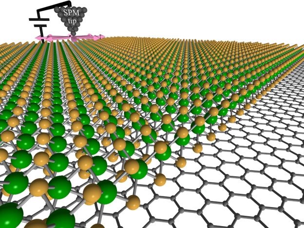 |
| Illustration depicts an autonomous experiment that directs an ultrasharp Scanning Probe Microscopy (SPM) tip throughout a 2D materials floor, capturing the native atomic and digital buildings. (Picture: Lawrence Berkeley Nationwide Laboratory)
|
|
The brand new methodology permits researchers to totally look at 2D surfaces. It affords a way of autonomous experimentation that’s quick and accessible. This opens the door to the detailed exploration of novel supplies, together with quantum supplies. The strategies and software program might be prolonged to different strategies in scanning probe microscopy. The researchers have summarized the tactic in a user-friendly, open entry, and tailorable software program package deal.
|
|
Two-dimensional materials methods are a lot wanted as a result of monumental purposeful section house spanning from insulating to conducting properties, which is pushed by atomic-scale and nanoscale defects that may be tuned by layer thickness, heterostructure stacking, twisting, and different strategies. Methods that present spectroscopic perception, equivalent to STM, are extraordinarily vital for researchers correlating nano faulty states with macroscopic properties.
|
|
Nonetheless, whereas hyperspectral scanning tunneling spectroscopy imaging supplies important perception into heterogenous digital properties on the atomic scale, its evaluation is impeded by the big time required. As an illustration, a hyperspectral optical map collected at 10 minutes per level in a 150 by 150-pixel grid would take effectively over one month to investigate.
|
|
The analysis workforce at Lawrence Berkeley Nationwide Laboratory’s Molecular Foundry, a Division of Power Workplace of Science person facility, developed a way of performing spatially dense, level spectroscopic measurements with an STM together with AI and ML. This strategy supplies sooner and extra correct statistically averaged knowledge that map and establish spectroscopic signatures of heterogeneous surfaces.
|
|
Utilizing tungsten disulfide (WS2) and gold (Au-111) surfaces as a benchmark, the workforce demonstrated methods to carry out measurements with reproducible ensuing spectra and methods to create statistically vital digital construction characterization of the totally different intrinsic defects that may be discovered on samples of curiosity.
|

