| Mar 21, 2024 |
|
(Nanowerk Information) A NIMS analysis staff has developed the world’s first n-channel diamond MOSFET (metal-oxide-semiconductor field-effect transistor). The developed n-channel diamond MOSFET gives a key step towards CMOS (complementary metal-oxide-semiconductor: probably the most fashionable applied sciences within the laptop chip) built-in circuits for harsh-environment- functions in addition to the event of diamond energy electronics.
|
|
This analysis was printed in Superior Science (“Excessive-temperature and high-electron mobility metal-oxide-semiconductor field-effect transistors based mostly on n-type diamond”).
|
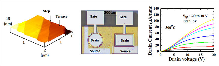 |
| World’s First N-Channel Diamond Subject-Impact Transistor: (Left) Atomic drive microscope picture of diamond epilayer floor morphology. (Center) Optical microscope picture of the diamond MOSFET. (Proper) Efficiency of the MOSFET measured at 300 °C. The drain present elevated when the gate voltage (Vg) was elevated from -20 V (indicated by a black line) to 10 V (indicated by a yellow line). (Picture: NIMS)
|
|
Semiconductor diamond has excellent bodily properties comparable to extremely wide-bandgap power of 5.5 eV, excessive carriers mobilities, and excessive thermal conductivity and many others, which is promising for the functions below excessive environmental circumstances with excessive efficiency and excessive reliability, such because the environments of excessive temperatures and excessive ranges of radiation (e.g., in proximity to nuclear reactor cores).
|
|
By utilizing diamond electronics, not solely can the thermal administration demand for typical semiconductors be alleviated however these gadgets are additionally extra power environment friendly and might endure a lot larger breakdown voltages and harsh environments. Then again, with the event of diamond progress applied sciences, energy electronics, spintronics, and microelectromechanical system (MEMS) sensors operatable below high-temperature and strong-radiation circumstances, the demand for peripheral circuitry based mostly on diamond CMOS gadgets has elevated for monolithic integration. For the fabrication of CMOS built-in circuits, each p- and n-type channel MOSFETs are required as these required for typical silicon electronics. Nonetheless, n-channel diamond MOSFETs had but to be developed.
|
|
This NIMS analysis staff developed a method to develop high-quality monocrystalline n-type diamond semiconductors with easy and flat terraces on the atomic stage by doping diamond with a low focus of phosphorus (diagram on the left within the determine above).
|
|
Utilizing this method, the staff succeeded in fabricating an n-channel diamond MOSFET for the primary time on this planet. This MOSFET consists primarily of an n-channel diamond semiconductor layer atop one other diamond layer doped with a excessive focus of phosphorus (center diagram within the determine). The usage of the latter diamond layer considerably lowered supply and drain contact resistance.
|
|
The staff confirmed that the fabricated diamond MOSFET truly functioned as an n-channel transistor. As well as, the staff verified the superb high-temperature efficiency of the MOSFET as indicated by its field-effect mobility—an necessary transistor efficiency indicator—of roughly 150 cm2/V・sec at 300 °C (graph on the best within the determine above).
|
|
4. These achievements are anticipated to facilitate the event of CMOS built-in circuits for the manufacture of energy-efficient energy electronics, spintronic gadgets and (MEMS) sensors below harsh environments.
|
